(Singapore)


Product Summary
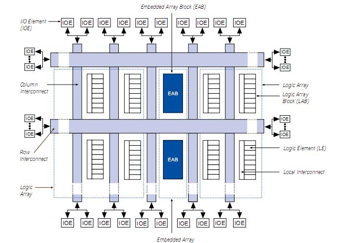
The EP1K30TC144-1N is a Programmable Logic Device. It provides a die-efficient, low-cost architecture by combining look-up table (LUT) architecture with EABs. The EP1K30TC144-1N is suitable for complex logic functions and memory functions such as digital signal processing, wide data-path manipulation, data transformation and microcontrollers, as required in high-performance communications applications. Based on reconfigurable CMOS SRAM elements, the EP1K30TC144-1N architecture incorporates all features necessary to implement common gate array megafunctions, along with a high pin count to enable an effective interface with system components.
Parametrics
EP1K30TC144-1N absolute maximum ratings: (1)Supply voltage With respect to ground:–0.5 to 3.6 V, –0.5 to 4.6 V; (2)DC input voltage:–2.0 to 5.75 V; (3)DC output current, per pin:–25 to 25 mA; (4)Storage temperature:–65℃ to 150℃; (5)Ambient temperature:–65℃ to 135℃; (6)Junction temperature:135℃.
Features
EP1K30TC144-1N features: (1)MultiVoltTM I/O pins can drive or be driven by 2.5-V, 3.3-V, or 5.0-V devices; (2)Low power consumption; (3)Bidirectional I/O performance (setup time [tSU] and clock-to-output delay [tCO]) up to 250 MHz; (4)Fully compliant with the peripheral component interconnect Special Interest Group (PCI SIG) PCI Local Bus Specification, Revision 2.2 for 3.3-V operation at 33 MHz or 66 MHz; (5)Cost-optimized process; (6)Low cost solution for high-performance communications applications; (7)Enhanced embedded array for implementing megafunctions such as efficient memory and specialized logic functions ; (8)Dual-port capability with up to 16-bit width per embedded array block (EAB); (9)Logic array for general logic functions; (10)Operate with a 2.5-V internal supply voltage; (11)In-circuit reconfigurability (ICR) via external configuration devices, intelligent controller, or JTAG port; (12)ClockLockTM and ClockBoostTM options for reduced clock delay, clock skew, and clock multiplication; (13)Built-in, low-skew clock distribution trees; (14)100% functional testing of all devices; test vectors or scan chains are not required; (15)Pull-up on I/O pins before and during configuration.
Diagrams
| Image | Part No | Mfg | Description |  |
Pricing (USD) |
Quantity | ||||||
|---|---|---|---|---|---|---|---|---|---|---|---|---|
 |
 EP1K30TC144-1N |
|
IC ACEX 1K FPGA 30K 144-TQFP |
Data Sheet |
|
|
||||||
| Image | Part No | Mfg | Description | |
Pricing (USD) |
Quantity | ||||||
 |
EP1K100FC256-1 |
|
IC ACEX 1K FPGA 100K 256-FBGA |
Data Sheet |
|
|
||||||
|
EP1K100FC256-1N |
|
IC ACEX 1K FPGA 100K 256-FBGA |
Data Sheet |
|
|
||||||
|
EP1K100FC256-2 |
|
IC ACEX 1K FPGA 100K 256-FBGA |
Data Sheet |
|
|
||||||
|
EP1K100FC256-2N |
|
IC ACEX 1K FPGA 100K 256-FBGA |
Data Sheet |
|
|
||||||
|
EP1K100FC256-3 |
|
IC ACEX 1K FPGA 100K 256-FBGA |
Data Sheet |
|
|
||||||
|
EP1K100FC256-3N |
|
IC ACEX 1K FPGA 100K 256-FBGA |
Data Sheet |
|
|
||||||