(Singapore)

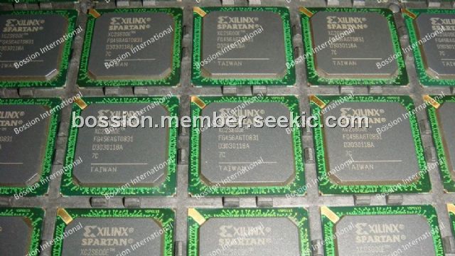
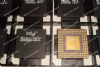
Product Summary
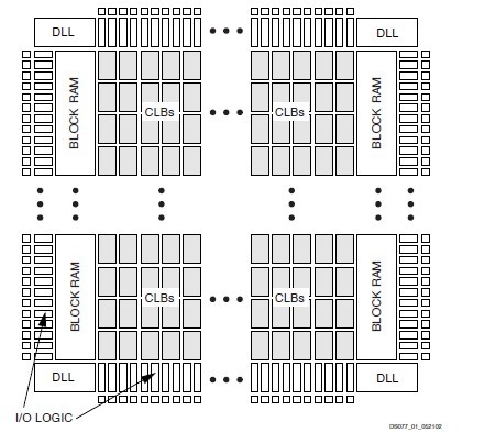
The XC2S600E-7FG456C is a Spartan-IIE FPGA. It has a regular, flexible, programmable architecture of Configurable Logic Block (CLB), surrounded by a perimeter of programmable Input/Output Blocks (IOBs). There are four Delay-Locked Loops (DLLs), one at each corner of the die. Two columns of block RAM lie on opposite sides of the die, between the CLBs and the IOB columns. The XC2S600E-7FG456C has six columns of block RAM. These functional elements are interconnected by a powerful hierarchy of versatile routing channels. The XC2S600E-7FG456C is customized by loading configuration data into internal static memory cells. Unlimited reprogramming cycles are possible with this approach. Stored values in these cells determine logic functions and interconnections implemented in the FPGA.
Parametrics
XC2S600E-7FG456C absolute maximum ratings: (1)Supply voltage relative to GND:–0.5V to 2.0V; (2)Supply voltage relative to GND:–0.5V to 4.0V; (3)Input reference voltage:–0.5V to 4.0V; (4)Storage temperature (ambient):–65℃ to +150℃; (5)Junction temperature:+125℃.
Features
XC2S600E-7FG456C features: (1)Densities as high as 15552 logic cells with up to 600,00 system gates; (2)Streamlined features based on Virtex FPGA architecture; (3)Unlimited reprogrammability; (4)Very low cost; (5)Cost-effective 0.15 micron process; (6)Fully PCI compliant; (7)Low-power segmented routing architecture; (8)Full readback ability for verification/observability; (9)Dedicated carry logic for high-speed arithmetic; (10)Efficient multiplier support; (11)Cascade chain for wide-input functions; (12)Abundant registers/latches with enable, set, reset; (13)Four dedicated DLLs for advanced clock control; (14)Four primary low-skew global clock distribution nets; (15)EEE 1149.1 compatible boundary scan logic; (16)Pb-free package options; (17)Low-cost packages available in all densities; (18)Family footprint compatibility in common packages; (19)19 high-performance interface standards; (20)Hot swap Compact PCI friendly; (21)Zero hold time simplifies system timing.
Diagrams
 |
 XC2S100 |
Other |
|
Data Sheet |
Negotiable |
|
||||||
|
XC2S100-5FG256C |
|
IC FPGA 2.5V 600 CLB'S 256-FBGA |
Data Sheet |
|
|
||||||
|
XC2S100-5FG256I |
|
IC FPGA 2.5V I-TEMP 256-FBGA |
Data Sheet |
|
|
||||||
 |
XC2S100-5FG456C |
|
IC FPGA 2.5V 600 CLB'S 456-FBGA |
Data Sheet |
|
|
||||||
|
XC2S100-5FG456I |
|
IC FPGA 2.5V I-TEMP 456-FBGA |
Data Sheet |
Negotiable |
|
||||||
|
XC2S100-5FGG256C |
|
IC SPARTAN-II FPGA 100K 256-FBGA |
Data Sheet |
|
|
||||||