(Singapore)


Product Summary
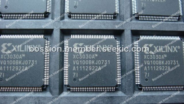
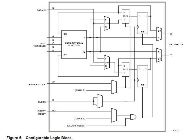
The XC3030A-7VQ100I is a Field Programmable Gate Array (FPGA). It provides a group of high-performance, high-density, digital integrated circuit. Their regular, extendable, flexible, user-programmable array architecture is composed of a configuration program store plus three types of configurable elements: a perimeter of I/O Blocks (IOBs), a core array of Configurable Logic Bocks (CLBs) and resources for interconnection. The development system of XC3030A-7VQ100I provides schematic capture and auto place-and-route for design entry. Logic and timing simulation, and in-circuit emulation are available as design verification alternatives. The design editor is used for interactive design optimization, and to compile the data pattern that represents the configuration program. The companion XC3030A-7VQ100I Configuration PROMs provide a very simple serial configuration program storage in a one-time programmable package. The XC3030A-7VQ100I Field Programmable Gate Array families provide a variety of logic capacities, package styles, temperature ranges and speed grades.
Parametrics
XC3030A-7VQ100I absolute maximum ratings: (1)VCC, Supply voltage relative to GND: –0.5 to +7.0 V; (2)VIN, Input voltage with respect to GND: –0.5 to VCC +0.5 V; (3)VTS, Voltage applied to 3-state output: –0.5 to VCC +0.5 V; (4)TSTG, Storage temperature (ambient): –65 to +150℃; (5)TSOL, Maximum soldering temperature (10 s @ 1/16 in.): +260℃; (6)TJ, Junction temperature plastic: +125℃; Junction temperature ceramic: +150℃.
Features
XC3030A-7VQ100I features: (1)Replaces TTL, MSI, and other PLD logic; (2)Integrates complete sub-systems into a single package; (3)Avoids the NRE, time delay, and risk of conventional masked gate arrays; (4)Guaranteed toggle rates of 70 to 370 MHz, logic delays from 7 to 1.5 ns; (5)System clock speeds over 85 MHz; (6)Low quiescent and active power consumption; (7)Compatible arrays ranging from 1,000 to 7,500 gate complexity; (8)Extensive register, combinatorial, and I/O capabilities; (9)High fan-out signal distribution, low-skew clock nets; (10)Internal 3-state bus capabilities; (11)TTL or CMOS input thresholds; (12)On-chip crystal oscillator amplifier.
Diagrams
 |
 XC3000 |
Other |
|
Data Sheet |
Negotiable |
|
||||
|
XC3000A |
Other |
|
Data Sheet |
Negotiable |
|
||||
|
XC3000L |
Other |
|
Data Sheet |
Negotiable |
|
||||
|
XC3020A-7PC84C |
|
IC LOGIC CL ARRAY 2000GAT 84PLCC |
Data Sheet |
Negotiable |
|
||||
 |
XC3030-100PC44C |
|
IC LOGIC CL ARRAY 3000GAT 44PLCC |
Data Sheet |
Negotiable |
|
||||
|
XC3030-100PC68C |
|
IC LOGIC CL ARRAY 3000GAT 68PLCC |
Data Sheet |
Negotiable |
|
||||