(Singapore)


Product Summary
The XC5206-5PQ160I is a Field-Programmable Gate Array. It is engineered to deliver low cost. Building on experiences gained with three previous successful SRAM FPGA families, the XC5206-5PQ160I brings a robust feature set to programmable logic design. The VersaBlock logic module, the VersaRing I/O interface, and a rich hierarchy of interconnect resources combine to enhance design flexibility and reduce time-to-market. Complete support for the XC5206-5PQ160I is delivered through the familiar Xilinx software environment. The XC5206-5PQ160I is fully supported on popular workstation and PC platforms. Popular design entry methods are fully supported, including ABEL, schematic capture, VHDL, and Verilog HDL synthesis. Designers utilizing logic synthesis can use their existing tools to design with the XC5206-6PQ100C.
Parametrics
XC5206-5PQ160I absolute maximum ratings: (1)VCC, Supply voltage relative to GND: -0.5 to +7.0 V; (2)VIN, Input voltage with respect to GND: -0.5 to VCC+0.5 V; (3)VTS, Voltage applied to 3-state output: -0.5 to VCC+0.5 V; (4)TSTG, Storage temperature (ambient): -65 to +150℃; (5)TSOL, Maximum soldering temperature (10 s @ 1/16 in. = 1.5 mm): +260℃; (6)TJ, Junction temperature in plastic packages: +125℃; (7)Junction temperature in ceramic packages: +150℃.
Features
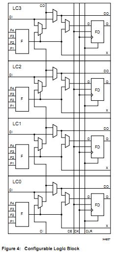
XC5206-5PQ160I features: (1)Low-cost, register/latch rich, SRAM based reprogrammable architecture: 0.5μm three-layer metal CMOS process technology; 256 to 1936 logic cells (3,000 to 23,000 gates); Price competitive with Gate Arrays; (2)System performance beyond 50 MHz; (3)6 levels of interconnect hierarchy; (4)VersaRing I/O Interface for pin-locking; (5)Dedicated carry logic for high-speed arithmetic functions; (6)Cascade chain for wide input functions; (7)Built-in IEEE 1149.1 JTAG boundary scan test circuitry on all I/O pins; (8)Internal 3-state bussing capability; (9)Four dedicated low-skew clock or signal distribution nets; (10)Versatile I/O and Packaging; (11)Innovative VersaRing I/O interface provides a high logic cell to I/O ratio, with up to 244 I/O signals; (12)Programmable output slew-rate control maximizes performance and reduces noise; (13)Zero Flip-Flop hold time for input registers simplifies system timing; (14)Independent Output Enables for external bussing; (15)Footprint compatibility in common packages within the XC5200 Series and with the XC4000 Series; (16)Over 150 device/package combinations, including advanced BGA, TQ, and VQ packaging available; (17)Fully Supported by Xilinx Development System; (18)Automatic place and route software; (19)Wide selection of PC and Workstation platforms; (20)Over 100 3rd-party Alliance interfaces; (21)Supported by shrink-wrap Foundation software.
Diagrams
 |
 XC5200 |
Other |
|
Data Sheet |
Negotiable |
|
||||
|
XC5200 Series |
Other |
|
Data Sheet |
Negotiable |
|
||||
|
XC5202-5PQ100C |
|
IC - FPGA SPEED GRADE 5 COM TEMP |
Data Sheet |
Negotiable |
|
||||
|
XC5202-6PC84C |
|
IC FPGA 64 CLB'S 84-PLCC |
Data Sheet |
Negotiable |
|
||||
|
XC5202-6PQ100C |
|
IC FPGA 64 CLB'S 100-PQFP |
Data Sheet |
Negotiable |
|
||||
|
XC5204-5PC84C |
|
IC FPGA 120 CLB'S 84-PLCC |
Data Sheet |
Negotiable |
|
||||